Design of a Hybrid 4th order Linkwitz-Riley Crossover Filter
Authors
Affiliation
Sriram Repaka
Hochschule Bremen
Mula Vishnu Veeranjan Sunkari
Hochschule Bremen
Published
July 15, 2026
1 Abstract
In this development report the design process of the Hybrid Linkwitz-Riley 4 crossover Filter is described. The development was done in a docker image for integrated circuit design, which is part of an open-source kit. The subject of this development report is the design of a crossover filter, including the filter characterization and several steps of circuit design. Furthermore, the layout process is also part of this documentation. Additionally, the experiences with the open source development environment are shared as well. The filter was designed by the use of the IHP sg13g2 PDK. GitHub Repo
2 Introduction
Integrated circuits (ICs) have become indispensable in modern electronic systems owing to their compact form factor and reduced power consumption relative to discrete implementations, like PCBs. In this work, we present the design and implementation of a Hybrid Linkwitz-Riley 4 Crossover filter using open-source tools, such as Xschem. The following documentation details the methodologies and development steps undertaken throughout the filter’s implementation.
This project is part of the Electronics Engineering (M. Sc.) course “Microelectronic Circuit Design (MCD)” at Hochschule Bremen City University of Applied Sciences (HSB).
The outcomes of this report and the development methodology used to design the filter will be made publicly available on GitHub. Everyone is welcome to use, modify, and share this work freely. This course and project would not have been possible without the excellent open-source tools created by the dedicated community of layout designers, enthusiasts, and developers. Some of the tools used include iic-osic-tools, IHP Open PDK, Docker, Xschem, ngspice, LTspice, Quarto, Python, and Git for version control.
3 Filter Specifications
The filter consists of two distinct topology types, each realized using operational amplifiers (OpAmps):
Low-Pass (LP)
High-Pass (HP)
In this project, a fully integrated fourth-order Hybrid Linkwitz-Riley Crossover Filter is designed, whose key specifications are given in Table 1 :
Table 1: Component selection parameters for the Linkwitz-Riley four-stage filter.
Parameter
Symbol
Target Value
Center Frequency(Center frequency of the narrowband response)
\(f_0\)
10 KHz
Quality Factor(Determines selectivity and sharpness)
\(Q\)
0.707(Butterworth Response)
DC Pass-Band Gain(Peak gain of unity at low frequencies)
\(H_0\)
~1
These parameters ensure a narrowband response around 10 kHz with a peak gain of unity at low frequencies and a sharp roll-off in the stop-bands.
4 Behavioural Model Design
As part of the initial design process, a behavioural model of the operational amplifier was developed and simulated. This model was used to study the basic functionality of the op amp before moving toward a more detailed transistor-level implementation.
The schematic of the operational amplifier was designed using LTspice, a freely available circuit simulation tool. LTspice was used to build the behavioural representation of the op amp, verify its operation, and observe its response under different simulation conditions. This step helped in understanding the expected behaviour of the circuit and provided a useful reference for the later stages of the filter design.
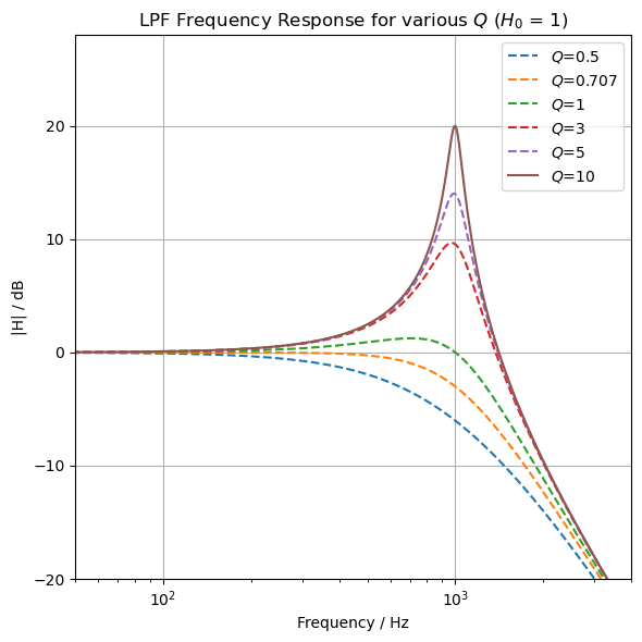
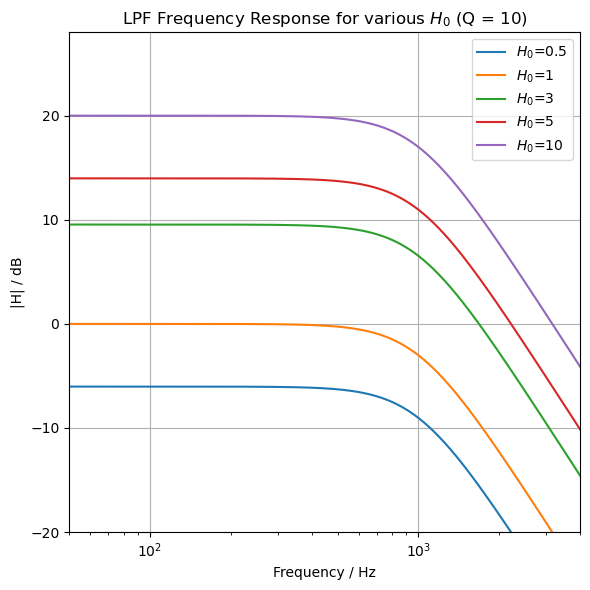
Determining Suitable Quality Factor
import numpy as npimport matplotlib.pyplot as plt# converterdef mag2db(H):return20*np.log10(np.abs(H))# Low-Pass transfer functiondef HLP(s, w0=2*np.pi*1000, Q=10, H0=1):return H0 / (1+ s/(w0*Q) + (s/w0)**2)# Specsf0 =1000# Hzw0 =2*np.pi*f0 # rad/sfreqs = np.linspace(1, 100*f0, 10000) # 1 Hz to 100 kHzs =1j*2*np.pi*freqsQs = [0.5, 0.707, 1, 3, 5, 10]H0_vals = [0.5, 1, 3, 5, 10]# Figure 1: LPF for different Qs (H0 = 1)plt.figure(figsize=(6,6))for Q in Qs: H = HLP(s, w0, Q, H0=1) style ='-'if Q==10else'--' plt.semilogx(freqs, mag2db(H), style, label=f'$Q$={Q}')plt.title('LPF Frequency Response for various $Q$ ($H_0$ = 1)')plt.xlabel('Frequency / Hz')plt.ylabel('|H| / dB')plt.grid(True)plt.xlim(50, 4000)plt.ylim(-20, 28)#plt.legend(loc='lower center', ncol=len(Qs), bbox_to_anchor=(0.5, -0.2))plt.legend()plt.tight_layout()# Figure 2: LPF for different H_0 (Q = 0.707)plt.figure(figsize=(6,6))for H0 in H0_vals: H = HLP(s, w0, 0.707, H0) plt.semilogx(freqs, mag2db(H), '-', label=f'$H_0$={H0}')plt.title('LPF Frequency Response for various $H_0$ (Q = 10)')plt.xlabel('Frequency / Hz')plt.ylabel('|H| / dB')plt.grid(True)plt.xlim(50, 4000)plt.ylim(-20, 28)#plt.legend(loc='lower center', ncol=len(H0_vals), bbox_to_anchor=(0.5, -0.2))plt.legend()plt.tight_layout()plt.show()
4.1 LTspice Behavioural Model Schematic
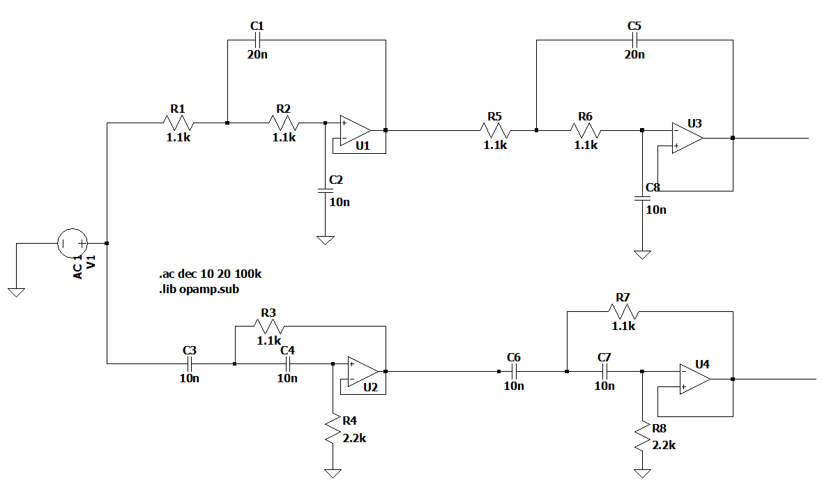
Figure 1: Behavioural model schematic of the LR4 filter designed in LTspice.
The behavioural model of the four stage Linkwitz Riley filter was designed and simulated in LTspice. The schematic Figure 1 consists of an AC voltage source, four active filter stages, and behavioural operational amplifier models. The input signal is applied using the voltage source V1, which is defined with an AC magnitude of 1 V. This allows the frequency response of the circuit to be directly observed in dB during AC analysis.
4.1.1 Mathematical Derivation
A standard Linkwitz-Riley 4th-order filter is constructed by cascading two identical 2nd-order Butterworth filters. The transfer function \(H(s)\) for the low-pass network can be expressed mathematically as:
\[H_{LP}(s) = \frac{1}{(s^2 + \sqrt{2}s + 1)^2}\]
Where the voltage gains of both cascading stages must match perfectly to maintain the ideal crossover characteristics.
4.1.2 Transfer Function and Filter Theory
The standard second-order low-pass transfer function is
where \(\omega_0\) is the natural angular frequency and \(Q\) is the quality factor.
The angular frequency is related to the cutoff frequency by
\[
\omega_0 = 2\pi f_c
\]
A fourth-order Linkwitz-Riley response can be obtained by cascading two identical second-order Butterworth sections. Therefore, the LR4 transfer function is
\[
H_{LR4}(s)=H_{BW2}(s)\cdot H_{BW2}(s)
\]
This produces a fourth-order response with a steeper roll-off compared with the second-order section.
4.2 Component Selection
The components chosen for the analog active operational amplifier implementation are summarized below.
Table 2: Component selection parameters for the active filter stage.
Component ID
Ideal Value
Chosen Value (Standard E96)
Tolerance
Function
\(R_1, R_2, R_3, R_5, R_6, R_7\)
\(1.1\text{ k}\Omega\)
\(1.1\text{ k}\Omega\)
\(1\%\)
Filter Node Resistors
\(R_4, R_8\)
\(2.2\text{ k}\Omega\)
\(2.2\text{ k}\Omega\)
\(1\%\)
Filter Node Resistors
\(C_1, C_5\)
\(20\text{ nF}\)
\(20\text{ nF}\)
\(5\%\)
Filter Node Capacitors
\(C_2, C_3, C_4, C_6, C_7, C_8\)
\(10\text{ nF}\)
\(10\text{ nF}\)
\(5\%\)
Filter Node Capacitors
\(U_1,U_2,U_3,U_4\)
OPA2134
OPA2134
—
Low-Noise Audio Op-Amp
As outlined in Table 2, standard resistor values are selected to match the ideal cutoff thresholds as closely as possible.
4.2.0.1 Low-Pass Section
For the second-order low-pass Sallen–Key stage, the natural frequency is determined using:
The component values (Table 2) used in the high-pass section are:
Component
Selected value
\(R_3\)
\(1.1\,\text{k}\Omega\)
\(R_4\)
\(2.2\,\text{k}\Omega\)
\(C_3\)
\(10\,\text{nF}\)
\(C_4\)
\(10\,\text{nF}\)
Substituting the selected values gives:
\[
f_0 \approx 10.23\,\text{kHz}
\]
and
\[
Q \approx 0.707.
\]
Therefore, both the low-pass and high-pass stages are designed with approximately the same natural frequency and Butterworth quality factor. Cascading two identical second-order stages in each branch produces the required fourth-order Linkwitz–Riley response.
4.3 LTspice AC Frequency Response
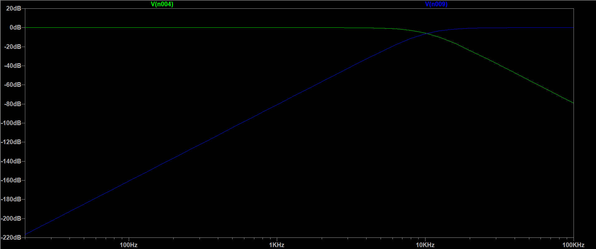
Figure 2: Behavioural model schematic of the LR4 filter designed in LTspice.
5 Principle of Operation: The 5-Transistor OTA (5T-OTA)
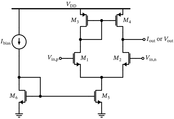
A 5-transistor operational transconductance amplifier (5T-OTA) Figure 3 is a fundamental analog building block designed to convert a differential input voltage into an output current (\(G = I_{\text{out}}/V_{\text{in}}\)). Unlike standard operational amplifiers that ideally feature zero output resistance, an OTA is characterized by a high output resistance. In practical integrated circuits, these devices are often loaded capacitively to create high-gain voltage amplifiers.
The internal operation of an NMOS-input 5T-OTA can be broken down into three distinct operational stages:
5.1 NMOS Differential Pair (\(M_1, M_2\))
The differential pair serves as the primary “input stage” that senses the incoming voltage signals.
Function:\(M_1\) and \(M_2\) are matched NMOS devices biased by the tail current flowing from \(M_5\). When a differential input voltage is applied across their gates, it is converted into differential drain currents governed by the transconductance (\(g_{\text{m}}\)) of the transistors (Pretl et al. 2026).
Symmetry: In an ideal, perfectly matched scenario, if the two input voltages are identical, the tail current (\(I_{\text{tail}}\)) splits exactly in half (\(I_{\text{tail}}/2\)) down both branches.
5.2 NMOS Tail Current Mirror (\(M_5, M_6\))
This stage establishes the stable DC biasing environment required for the entire amplifier circuit.
Function: Transistors \(M_5\) and \(M_6\) form a current mirror. An external reference current (\(I_{\text{bias}}\)) is fed through the transistor \(M_6\), which is then mirrored directly into \(M_5\)(Pretl et al. 2026).
The Tail Current:\(M_5\) operates as the tail current source, defining the total bias current (\(I_{\text{tail}}\)) that passes through the input differential pair. This tail current is a critical design parameter, as it directly sets both the transconductance (\(g_{\text{m}}\)) and the overall speed of the amplifier.
5.3 PMOS Current Mirror Load (\(M_3, M_4\))
This final section acts as an active load for the input pair and performs the differential-to-single-ended signal conversion.
Function: Transistors \(M_3\) and \(M_4\) form a PMOS current mirror. The diode-connected \(M_3\) senses the changing current flowing through the left branch (\(M_1\)) and replicates it over to the right branch via \(M_4\)(Pretl et al. 2026).
Summing at the Output: At the single-ended output node, the mirrored current from \(M_4\) and the direct current from the right input branch (\(M_2\)) are subtracted/summed. When this net signal current is forced into the high-impedance output node, it builds up the final output voltage.
5.4 Transistor Sizing and \(g_{\text{m}}/I_{\text{D}}\) Selection Strategy
In a 5T-OTA, selecting the device sizes involves balancing fundamental trade-offs between speed, power efficiency, noise, and matching. Rather than applying a uniform \(g_{\text{m}}/I_{\text{D}}\) ratio across all devices, each sub-block is targeted with a specific transconductance efficiency to maximize overall circuit performance.
For the input stage, a higher \(g_{\text{m}}/I_{\text{D}}\) value—typically in the range of 10 to 12 V⁻¹—is chosen to operate the devices in moderate inversion.
Gain and Power Efficiency
The primary goal of the input pair is to provide high transconductance (\(g_{\text{m}}\)) to maximize the amplifier’s gain. Biasing at a high \(g_{\text{m}}/I_{\text{D}}\) value achieves this required transconductance while consuming the absolute minimum current (\(I_{\text{D}}\)), maximizing power efficiency.
Noise and Offset Optimization
Maximizing the \(g_{\text{m}}/I_{\text{D}}\) ratio minimizes the overdrive voltage. This is a critical strategy for reducing the input offset voltage caused by threshold voltage mismatch between \(M_1\) and \(M_2\), while simultaneously minimizing the input-referred thermal noise (Nagulapalli et al. 2019).
5.4.2 2. PMOS Load (\(M_3, M_4\)) and NMOS Tail (\(M_5, M_6\)) Current Mirrors
For the current mirror and load network, a lower \(g_{\text{m}}/I_{\text{D}}\) value—typically in the range of 6 to 8 V⁻¹—is chosen to operate the devices in strong inversion.
Current Matching Accuracy
For current mirrors, matching accuracy takes priority over transconductance efficiency. A lower \(g_{\text{m}}/I_{\text{D}}\) ratio dictates a larger overdrive voltage (\(V_{\text{GS}} - V_{\text{th}}\)). This larger overdrive significantly reduces current mismatch arising from local threshold voltage variations (\(\Delta V_{\text{th}}\)) across the mirrors.
Output Resistance and DC Gain
Operating these current sources at a lower \(g_{\text{m}}/I_{\text{D}}\) alongside longer channel lengths maximizes their output resistance (\(r_0\)). This improves both the mirroring precision and the overall DC voltage gain of the OTA (Nagulapalli et al. 2019).
Noise Suppression
To reduce the total output noise contribution of the OTA, the transconductance of the load transistors (\(g_{\text{m3,4}}\)) must be kept significantly lower than the transconductance of the input pair (\(g_{\text{m1,2}}\)). Biasing the load devices at a lower \(g_{\text{m}}/I_{\text{D}}\) ensures their individual transconductance remains small, dropping their noise contribution (Nagulapalli et al. 2019).
5.4.3 3. Summary Sizing Targets and Trade-offs
The table below outlines the final targeted \(g_{\text{m}}/I_{\text{D}}\) configuration and the core trade-offs managing the 5T-OTA architecture, further narrowing the no of combinations. To streamline the simulation and optimization phase, the design space was restricted to tight \(g_{\text{m}}/I_{\text{D}}\) windows. This dramatically reduces the number of design permutations and sweeps required during circuit characterization.
Transistor Group
Inversion Region
Targeted \(g_{\text{m}}/I_{\text{D}}\) Value
Key Design Priorities
Input Pair (\(M_1, M_2\))
Moderate Inversion
10 to 12 V⁻¹
High gain, low power consumption, minimized offset.
PMOS Load (\(M_3, M_4\))
Strong Inversion
6 to 8 V⁻¹
Low noise contribution, high output resistance, and precise current matching.
NMOS Tail (\(M_5, M_6\))
Strong Inversion
6 to 8 V⁻¹
High output resistance for stable biasing and precise current replication.
5.4.4 Transistor Sizing and Architecture for the 5T-OTA
To determine the physical dimensions of the transistors within the 5T-OTA architecture, \(g_m/I_D\) design methodology utilizes pre-characterized technology lookup tables
5.4.5 Design Specification & Reference Parameters
The circuit dimensioning is driven by explicit performance targets, including bandwidth, capacitive loading, and transistor geometry constraints. The primary design inputs and initial assumptions are structured in Table 3.
Table 3: Input design parameters and specifications for the 5T-OTA as per sizing document in (Pretl et al. 2026).
The required transconductance for the differential input pair (\(M_{1/2}\)) is directly tied to the unity-gain bandwidth requirement of the system configuration. To protect against process, voltage, and temperature (PVT) variations, alongside parasitic transistor self-loading, a safety scaling factor of \(3\) is introduced into the fundamental bandwidth equation:
Substituting our core specifications (\(10\text{ MHz}\) and \(50\text{ fF}\)), the script calculates the necessary small-signal capability (Pretl et al. 2026):
To comply with standard layout grids and bias generation modules, this value is rounded up to a clean operational baseline of \(4.0\text{ }\mu\text{A}\) (\(I_{D1,2} = 2.0\text{ }\mu\text{A}\)) (Pretl et al. 2026).
5.4.6.3 Gate Voltage & Physical Width Mapping
Operating at a fixed length (\(L = 5\text{ }\mu\text{m}\)), the calculated current and target \((g_m/I_D)\) are mapped to the semiconductor technology databases to track their native gate-to-source voltage drops (\(V_{\mathrm{GS}}\)):
Using the technology-specific current density value per micrometer of transistor width (\(I_D/W\)) provided by the lookup tables at these operating points, the physical widths (\(W\)) are computed via:
To mirror the incoming off-chip reference current (\(20\text{ }\mu\text{A}\)) down to our internal tail target (\(4\text{ }\mu\text{A}\)), the geometry of the receiving diode-connected transistor (\(M_6\)) is scaled proportionally against the dimensions of \(M_5\):
The open-loop DC voltage gain (\(A_0\)) of a single-stage 5T-OTA is defined by the transconductance of the input pair relative to the combined output conductances (\(g_{\mathrm{ds}}\)) of both the input transistors and the active loads.
The total small-signal DC voltage gain is expressed using the following equation:
We can use the readly available sizing document to size a basic 5T-OTA, based on the input design parameters the document caculates the sizing for each transistor and other parameters like the gain, noise, power consumption and settling time. A sizing document is available at (Pretl et al. 2026)
5.5 Transition to a Two-Stage OTA Architecture
5.5.1 Why the 5T-OTA is Insufficient for Audio
While the basic 5T-OTA is simple and efficient, it is not suitable for an audio amplifier because its open-loop DC gain is only \(34.8\text{ dB}\) (around \(55\text{ V/V}\)). High-fidelity audio applications demand significantly more gain to minimize output distortion, and keep gain errors low.
Because a single transistor stage cannot provide enough amplification on its own, we must transition to a Two-Stage OTA architecture as suggested in (Pretl et al. 2026).
5.5.2 The Two-Stage Gain Equation
By cascading a second amplification stage directly after the initial differential stage, the total open-loop gain is multiplied together. The resulting total DC voltage gain is defined by the following equation:
\[A_{\mathrm{OL, total}} = A_{v1} \cdot A_{v2}\]
Where: \(A_{\mathrm{OL, total}}\) is the total open-loop DC gain of the system. \(A_{v1}\) is the voltage gain of the first stage (the differential input pair). \(A_{v2}\) is the voltage gain of the second stage (the common-source output stage).
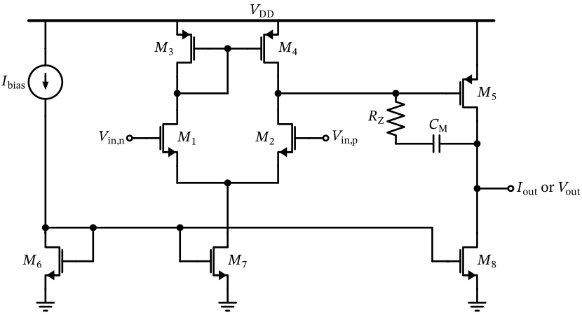
This structural change easily pushes the total gain into the desired range for audio quality, while the added Miller compensation network (\(C_\mathrm{M}\) and \(R_\mathrm{Z}\)) ensures the entire circuit remains stable.
5.6 Transistor Sizing and Architecture for the 2-Stage Miller OTA
Integral part of an Linkwitz-Riley 4 Crossover Filter is an amplifier, and a 2-stage OTA is a good option as it offers high gain and is begginer friendly design. A 2-stage OTA is essentially an 5-T OTA and a PMOS common source ampliflier cascaded with a Miller compensation capacitor \(C_{\text{M}}\) and a Null resistor \(R_{\text{Z}}\) as shown in Figure 4.
Figure 4: The 2-stage OTA.
There are 4 major aspects of this OTA the input differential pair, pmos current mirrors, output gain PMOS, and tail current NMOS’s. The sizing of these transistors is again done using gm/Id methodology.
5.6.1 2. Design Space Explorations: Component and Geometry Selection
To transition successfully to the two-stage architecture, two critical component adjustments were made to ensure loop stability and realistic system performance:
Upgrading \(C_{\mathrm{load}}\) to \(1\text{ pF}\) (from \(50\text{ fF}\)): A \(50\text{ fF}\) load only accounts for tiny, localized on-chip parasitics (Lenka et al. 2022). Since this OTA is designed to drive inside an LR4 active crossover filter network, \(1\text{ pF}\) was chosen to represent realistic load (Lenka et al. 2022).
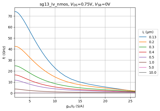
Scaling Down \(L\) to \(2\text{ }\mu\text{m}\) (from \(5\text{ }\mu\text{m}\)): Initial designs using \(L = 5\text{ }\mu\text{m}\) suffered from severe high-frequency oscillations near the roll-off frequency. The provided technology plot reveals that an \(L = 5\text{ }\mu\text{m}\) device features an extremely low transit frequency (\(f_{\mathrm{T}} < 1\text{ GHz}\)) as shown in the plot below. By scaling to \(L = 2\text{ }\mu\text{m}\), the internal device \(f_{\mathrm{T}}\) is pushed much higher (towards the \(2\text{ to } 3\text{ GHz}\) range as shown in the plot below at L=1), pushing parasitic non-dominant poles safely past our operating bandwidth and eliminating the oscillations.
To shield the circuit from high-frequency stability decay, a Miller capacitance (\(C_\mathrm{M}\)) is introduced relative to the total output load (Nagulapalli et al. 2019):
The input pair transconductance (\(g_{m1,2}\)) calculation incorporates a protective \(3\times\) multiplier scaling to safeguard the target bandwidth against local process tracking shifts:
Dividing by the efficiency parameter \((g_m/I_D)_{1,2} = 11\), the branch current yields a total ideal tail allocation of \(I_{\mathrm{tail,ideal}} \approx 17.14\text{ }\mu\text{A}\). Quantizing this to a regular layout grid (steps of \(0.5\text{ }\mu\text{A}\)) locks in our tail profile:
Tail Current Source (\(I_{\mathrm{tail}}\)):\(17.00\text{ }\mu\text{A}\)
True Branch Current (\(I_{D1,2}\)):\(8.50\text{ }\mu\text{A}\)
To guarantee a robust design, the secondary transconductance stage (\(M_5\)) must easily out-pace the target operational bandwidth boundary via \((g_m/I_D)\) sizing methodology:
Dividing this by its distinct parameter \((g_m/I_D)_5 = 10\) establishes the analytical current demand \(I_{D5,\mathrm{req}} = 13.823\text{ }\mu\text{A}\). Mirror scaling constraints align the true current flow down to exactly \(10.00\text{ }\mu\text{A}\) based on physical layout sizes. At this grid point, the driver generates its final small-signal capability:
The zero-nulling frequency compensation resistance (\(R_z\)) is set to cancel the right-half-plane (RHP) zero generated across the Miller framework (L. 2025):
The physical layout dimensions established by mapping the grid current data back to the pygmid database lookup functions are structured in Table 5.
Table 5: Final optimized structural dimensions for the 2-Stage Miller OTA.
Transistor Group
Geometric Layout Role
Width (\(W\))
Length (\(L\))
\(M_{1/2}\)
NMOS Input Differential Pair
\(2.5\text{ }\mu\text{m}\)
\(2\text{ }\mu\text{m}\)
\(M_{3/4}\)
PMOS Active First-Stage Load
\(3.5\text{ }\mu\text{m}\)
\(2\text{ }\mu\text{m}\)
\(M_5\)
PMOS Common-Source Output Driver
\(9.5\text{ }\mu\text{m}\)
\(2\text{ }\mu\text{m}\)
\(M_6\)
NMOS External Reference Bias Input Receiver
\(2.0\text{ }\mu\text{m}\)
\(2\text{ }\mu\text{m}\)
\(M_7\)
NMOS First-Stage Tail Current Mirror
\(1.5\text{ }\mu\text{m}\)
\(2\text{ }\mu\text{m}\)
\(M_8\)
NMOS Second-Stage Output Active Load
\(1.0\text{ }\mu\text{m}\)
\(2\text{ }\mu\text{m}\)
The sizing procedure and its calculation are best performed in a Jupyter notebook, as we can easily look up the exact data from the pre-computed lookup tables:
TipNotebook 2-Stage-OTA Sizing
# Sizing for a 2 Stage OTAfrom pygmid import Lookup as lkimport numpy as nplv_nmos = lk('sg13_lv_nmos.mat')lv_pmos = lk('sg13_lv_pmos.mat')# list of parameters: VGS, VDS, VSB, L, W, NFING, ID, VT, GM, GMB, GDS, CGG, CGB, CGD, CGS, CDD, CSS, STH, SFL# if not specified, minimum L, VDS=max(vgs)/2=0.9 and VSB=0 are used
# define the given parameters as taken from the specification table or inital guessesc_load =1e-12#c_load = 1e-12gm_id_m12 =11gm_id_m34 =7gm_id_m5 =10gm_id_m678 =6l_12 =2l_34 =2l_5 =2l_678 =2f_bw =10e6# -3dB bandwidth of the voltage bufferi_total_limit =30e-6i_bias_in =20e-6output_voltage =1.3vin_min =0.7vin_max =0.9vdd_min =1.45vdd_max =1.55gain =60
c_m_min =0.22*c_load# Industrial scaling multiplier (6.6x the lower bound) to swallow up local device parasiticsc_m =0.5*c_load#c_m = 150e-16#c_m = c_m_min
--- Step 3: Second Stage Stability-Driven Constraints ---
Required Minimum Stage 2 transconductance gm5 = 0.13823 mS
Analytically Required Stage 2 Bias Current    = 13.823 µA
# we calculate the first stage dc gaingm_gds_m12 = lv_nmos.lookup('GM_GDS', GM_ID=gm_id_m12, L=l_12, VDS=0.75, VSB=0)gm_gds_m34 = lv_pmos.lookup('GM_GDS', GM_ID=gm_id_m34, L=l_34, VDS=0.75, VSB=0)gds_m12 = gm_m12 / gm_gds_m12gm_m34 = gm_id_m34 * i_tail/2gds_m34 = gm_m34 / gm_gds_m34a0 = gm_m12 / (gds_m12 + gds_m34)print('First stage gain a0 =', round(20*np.log10(a0), 1), 'dB')
First stage gain a0 = 31.6 dB
# we can now look up the VGS of the MOSFETvgs_m12 = lv_nmos.look_upVGS(GM_ID=gm_id_m12, L=l_12, VDS=0.75, VSB=0.0)vgs_m34 = lv_pmos.look_upVGS(GM_ID=gm_id_m34, L=l_34, VDS=0.75, VSB=0.0) vgs_m76 = lv_nmos.look_upVGS(GM_ID=gm_id_m678, L=l_678, VDS=0.75, VSB=0.0) print('vgs_12 =', round(float(vgs_m12), 3), 'V')print('vgs_34 =', round(float(vgs_m34), 3), 'V')print('vgs_76 =', round(float(vgs_m76), 3), 'V')
vgs_12 = 0.37 V
vgs_34 = 0.617 V
vgs_76 = 0.547 V
# calculate all widthsid_w_m12 = lv_nmos.lookup('ID_W', GM_ID=gm_id_m12, L=l_12, VDS=vgs_m12, VSB=0)w_12 = id_m12 / id_w_m12w_12_round =max(round(w_12*2)/2, 0.5)print('M1/2 W =', round(w_12, 2), 'um, rounded W =', w_12_round, 'um')id_m34 = id_m12id_w_m34 = lv_pmos.lookup('ID_W', GM_ID=gm_id_m34, L=l_34, VDS=vgs_m34, VSB=0)w_34 = id_m34 / id_w_m34w_34_round =max(round(w_34*2)/2, 0.5) print('M3/4 W =', round(w_34, 2), 'um, rounded W =', w_34_round, 'um')id_w_m7 = lv_nmos.lookup('ID_W', GM_ID=gm_id_m678, L=l_678, VDS=vgs_m76, VSB=0)w_7 = i_tail / id_w_m7w_7_round =max(round(w_7*2)/2, 0.5)print('M7 W =', round(w_7, 2), 'um, rounded W =', w_7_round, 'um')w_6 = w_7_round * i_bias_in / i_tailw_6_round =max(round(w_6*2)/2, 0.5)print('M6 W =', round(w_6_round, 2), 'um')# ==============================================================================# Sizing for Second Stage: M8 and M5# ==============================================================================print('\n--- Second Stage Sizing ---')# Step A: Size M8 (Stage 2 NMOS Load Mirror) using id_m5_requiredid_w_m8 = lv_nmos.lookup('ID_W', GM_ID=gm_id_m678, L=l_678, VDS=0.75, VSB=0)w_8 = id_m5_required / id_w_m8w_8_round =max(round(w_8 *2) /2, 0.5)print('M8 W =', round(w_8, 2), 'um, rounded W =', w_8_round, 'um')# Step B: Realign true mirrored current to layout grid constraintsmirror_ratio_m8_m6 = w_8_round / w_6_roundid_m5 = i_bias_in * mirror_ratio_m8_m6print(f'True Mirrored Stage 2 Current (id_m5) = {id_m5/1e-6:.3f} µA')# Step C: Re-calculate actual physical gm5 and size M5 (PMOS Driver)gm_m5 = gm_id_m5 * id_m5id_w_m5 = lv_pmos.lookup('ID_W', GM_ID=gm_id_m5, L=l_5, VDS=0.75, VSB=0)w_5 = id_m5 / id_w_m5w_5_round =max(round(w_5 *2) /2, 0.5)print('M5 W =', round(w_5, 2), 'um, rounded W =', w_5_round, 'um')# Step D: Complete the flow with your Zero-Nulling Resistor valuerz =2/ gm_m5print(f'Textbook Zero-Nulling Resistor Rz = {rz/1e3:.2f} kΩ')
M1/2 W = 2.7 um, rounded W = 2.5 um
M3/4 W = 3.55 um, rounded W = 3.5 um
M7 W = 1.25 um, rounded W = 1.5 um
M6 W = 2.0 um

--- Second Stage Sizing ---
M8 W = 1.01 um, rounded W = 1.0 um
True Mirrored Stage 2 Current (id_m5) = 10.000 µA
M5 W = 9.27 um, rounded W = 9.5 um
Textbook Zero-Nulling Resistor Rz = 20.00 kΩ
# ==============================================================================# 5. Total Open-Loop DC Gain Evaluation# ==============================================================================print('\n--- Total DC Gain Evaluation ---')# Second stage gain evaluation# Extract the intrinsic gain of the PMOS Common-Source driver (M5)gm_gds_m5 = lv_pmos.lookup('GM_GDS', GM_ID=gm_id_m5, L=l_5, VDS=0.75, VSB=0)gds_m5 = gm_m5 / gm_gds_m5# Extract the output conductance density of the NMOS mirror load (M8)gds_id_m8 = lv_nmos.lookup('GDS_ID', GM_ID=gm_id_m678, L=l_678, VDS=0.75, VSB=0)gds_m8 = gds_id_m8 * id_m5# Compute Stage 2 Gaina1 = gm_m5 / (gds_m5 + gds_m8)# Compute Total Open-Loop Gaina0_total = a0 * a1print(f'Stage 1 Open-Loop Gain (A1) = {20*np.log10(a0):.1f} dB')print(f'Stage 2 Open-Loop Gain (A2) = {20*np.log10(a1):.1f} dB')print(f'Total Open-Loop Gain (A0) = {20*np.log10(a0_total):.1f} dB')gain_error = a0_total / (1+ a0_total)print('voltage gain error =', round((gain_error-1)*100, 1), '%')
--- Total DC Gain Evaluation ---
Stage 1 Open-Loop Gain (A1) = 31.6 dB
Stage 2 Open-Loop Gain (A2) = 34.3 dB
Total Open-Loop Gain (A0)   = 65.9 dB
voltage gain error = -0.1 %
# ==============================================================================# 6. Node Parasitic Extraction, Actual UGBW, and Final Summary# ==============================================================================print('--- Node Parasitic Extraction & Actual UGBW ---')# Look up frequency-dependent parasitic capsgm_cgs_m12 = lv_nmos.lookup('GM_CGS', GM_ID=gm_id_m12, L=l_12, VDS=0.75, VSB=0)gm_cdd_m12 = lv_nmos.lookup('GM_CDD', GM_ID=gm_id_m12, L=l_12, VDS=0.75, VSB=0)gm_cdd_m34 = lv_pmos.lookup('GM_CDD', GM_ID=gm_id_m34, L=l_34, VDS=0.75, VSB=0)# NEW: Look up the gate-capacitance of the M5 drivergm_cgg_m5 = lv_pmos.lookup('GM_CGG', GM_ID=gm_id_m5, L=l_5, VDS=0.75, VSB=0)gm_w_m34 = lv_pmos.lookup('GM_W', GM_ID=gm_id_m34, L=l_34, VDS=0.75, VSB=0)gm_m34 = gm_w_m34 * w_34_round# NEW: Add the M5 gate load to the total internal node parasitic calculationc_para_internal =abs(gm_m12 / gm_cgs_m12) +abs(gm_m12 / gm_cdd_m12) +abs(gm_m34 / gm_cdd_m34) +abs(gm_m5 / gm_cgg_m5)# The effective Miller capacitance includes this parallel parasitic loadingc_m_eff = c_m + c_para_internal# Calculate the actual physical UGBW roll-off from the true c_m_efff_bw_actual = gm_m12 / (2* np.pi * c_m_eff)t_slew = c_m_eff*output_voltage / i_tailprint('slewing time =', round(t_slew/1e-6, 3), 'µs')tau =1/ (2* np.pi * f_bw_actual)t_settle =5* tauprint('settling time =', round(t_settle/1e-6, 3), 'µs')print(f'Internal Node Parasitic Load = {c_para_internal/1e-15:.2f} fF and of which m5 {abs(gm_m5 / gm_cgg_m5)/1e-15}')print(f'Effective Miller Capacitance = {c_m_eff/1e-15:.2f} fF')i_total_rail = i_bias_in + i_tail + id_m5# Power calculation at the minimum and maximum VDD limitspower_dissipation_min = i_total_rail * vdd_minpower_dissipation_max = i_total_rail * vdd_maxprint(f"Total Current from VDD Rail = {i_total_rail/1e-6:.2f} µA")# ==============================================================================# 7. Final Industrial Sizing Blueprint Summary Printout# ==============================================================================cap_density =1.5e-15w_cm_approx = np.sqrt(c_m / cap_density)print('\n============================================================')print(' Textbook-Aligned Industrial 2-Stage Miller OTA Blueprint')print('============================================================')print('\nManufactured Device Sizes:')print(f' M1/2 W = {w_12_round} µm, L = {l_12} µm [NMOS Input Pair]')print(f' M3/4 W = {w_34_round} µm, L = {l_34} µm [PMOS Active Load]')print(f' M5 W = {w_5_round} µm, L = {l_5} µm [PMOS CS Driver]')print(f' M6 W = {w_6_round} µm, L = {l_678} µm [NMOS Ref Mirror]')print(f' M7 W = {w_7_round} µm, L = {l_678} µm [NMOS Tail Mirror]')print(f' M8 W = {w_8_round} µm, L = {l_678} µm [NMOS Load Mirror]')print('\nPassives Allocation:')print(f' Miller Cap Cm = {c_m/1e-15:.1f} fF ({w_cm_approx:.1f} x {w_cm_approx:.1f} µm MOM cap)')print(f' Nulling Resistor Rz = {rz/1e3:.2f} kΩ')print('\nEvaluated Performance Metrics:')print(f' Target Specification UGBW = {f_bw/1e6:.2f} MHz')print(f' Actual Predicted UGBW = {f_bw_actual/1e6:.2f} MHz (including layout parasitics)')print(f' Stage 1 Open-Loop Gain A1 = {20*np.log10(a0):.1f} dB')print(f' Stage 2 Open-Loop Gain A2 = {20*np.log10(a1):.1f} dB')print(f' Total Open-Loop Gain A0 = {20*np.log10(a0_total):.1f} dB (Specification: >= {gain} dB)')print('\nCurrent Consumption Budget:')print(f' Stage 1 Tail Branch (I_tail) = {i_tail/1e-6:.2f} µA')print(f' Stage 2 Core Branch (Id_M5) = {id_m5/1e-6:.2f} µA')print(f' Total Net Core Current Draw = {(i_tail + id_m5)/1e-6:.2f} µA (Limit Budget: <= {i_total_limit/1e-6:.2f} µA)')print(f" Power Dissipation (at VDD = {vdd_max}V) = {power_dissipation_max*1e6:.2f} µW")print('============================================================')
--- Node Parasitic Extraction & Actual UGBW ---
slewing time = 0.046 µs
settling time = 0.032 µs
Internal Node Parasitic Load = 99.54 fF and of which m5 80.75863693703191
Effective Miller Capacitance = 599.54 fF
Total Current from VDD Rail = 47.00 µA

============================================================
  Textbook-Aligned Industrial 2-Stage Miller OTA Blueprint
============================================================

Manufactured Device Sizes:
  M1/2  W = 2.5 µm,  L = 2 µm   [NMOS Input Pair]
  M3/4  W = 3.5 µm,  L = 2 µm   [PMOS Active Load]
  M5    W = 9.5 µm,  L = 2 µm   [PMOS CS Driver]
  M6    W = 2.0 µm,  L = 2 µm   [NMOS Ref Mirror]
  M7    W = 1.5 µm,  L = 2 µm   [NMOS Tail Mirror]
  M8    W = 1.0 µm,  L = 2 µm   [NMOS Load Mirror]

Passives Allocation:
  Miller Cap Cm       = 500.0 fF (18.3 x 18.3 µm MOM cap)
  Nulling Resistor Rz = 20.00 kΩ

Evaluated Performance Metrics:
  Target Specification UGBW = 10.00 MHz
  Actual Predicted UGBW     = 24.82 MHz (including layout parasitics)
  Stage 1 Open-Loop Gain A1 = 31.6 dB
  Stage 2 Open-Loop Gain A2 = 34.3 dB
  Total Open-Loop Gain A0   = 65.9 dB (Specification: >= 60 dB)

Current Consumption Budget:
  Stage 1 Tail Branch (I_tail) = 17.00 µA
  Stage 2 Core Branch (Id_M5)  = 10.00 µA
  Total Net Core Current Draw  = 27.00 µA (Limit Budget: <= 30.00 µA)
  Power Dissipation (at VDD = 1.55V) = 72.85 µW
============================================================
By splitting the design across cascaded active blocks, the total system gain successfully clears the targets required. The cumulative performance metrics are detailed in Table 6.
Table 6: Performance summary of the 2-Stage Miller OTA configuration.
Performance Metric
Design Value
Status / Constraint
Stage 1 Gain (\(A_1\))
\(31.6\text{ dB}\)
Primary Voltage Boost
Stage 2 Gain (\(A_2\))
\(34.3\text{ dB}\)
Secondary Common-Source Boost
Total Open-Loop Gain (\(A_0\))
\(65.9\text{ dB}\)
Passed (\(\ge 60\text{ dB}\) Target)
**Voltage Gain Error
\(-0.1\%\)
Passes a target of \(<0.3%\)
Core Branch Current Draw
\(27.00\text{ }\mu\text{A}\)
Passed (\(\le 30.00\text{ }\mu\text{A}\) Budget)
Peak Power Dissipation
\(72.85\text{ }\mu\text{W}\)
Simulated at \(V_{\mathrm{DD,max}} = 1.55\text{ V}\)
Predicted Layout UGBW
\(24.82\text{ MHz}\)
Exceeds \(10\text{ MHz}\) baseline specification
5.7 2-Stage OTA Simulation Framework and Results
To validate the analytical sizing derivations and empirical stability optimizations, the design was constructed and verified inside the Xschem schematic capture environment utilizing the IHP SG13G2 open-source PDK.
5.7.1 Simulation Environment Setup
The core amplifier design and its folders :
ota-2stage.sch & ota-2stage.sym: The fundamental schematic and corresponding symbol containing the optimized geometric sizing (e.g., \(L = 2\text{ }\mu\text{m}\), \(C_{\mathrm{M}} = 0.9\text{ pF}\), and \(R_{\mathrm{z}} = 24\text{ k}\Omega\)).
To evaluate the design against all primary performance metrics, three separate testbenches were built in the same workspace folder:
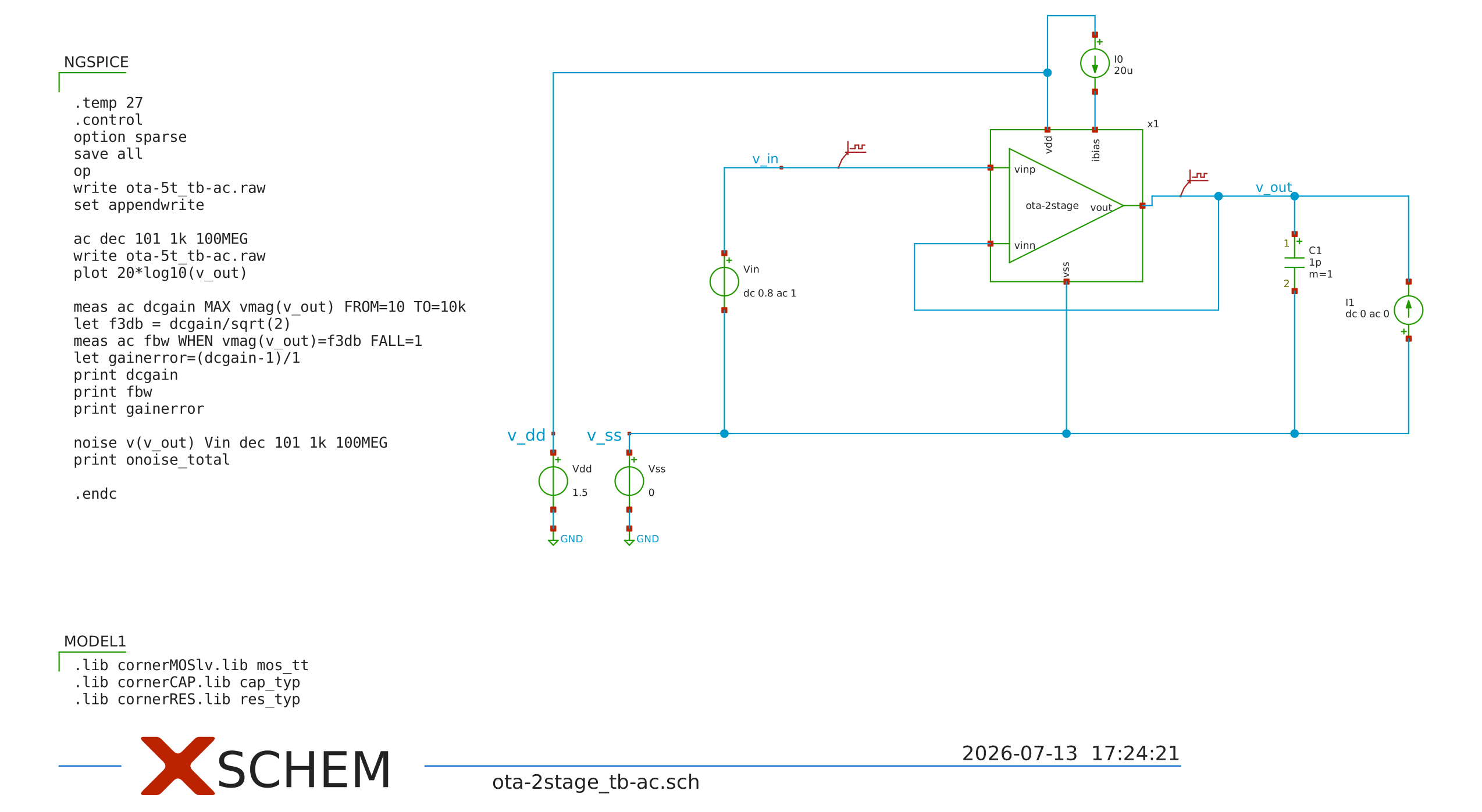
ota-2stage_tb-ac.sch: Small-signal AC analysis to characterize closed-loop DC gain (\(A_0\)), and Unity-Gain Bandwidth (\(f_(bw)\)) as shown in Figure 5.
ota-2stage_tb-trans.sch: Transient analysis to verify step-response behavior and settling time.
The simulation runs verified that the optimized pole-splitting configuration successfully resolves the high-frequency stability challenges encountered in early design cycles.
5.7.2.1 1. Small-Signal AC Response
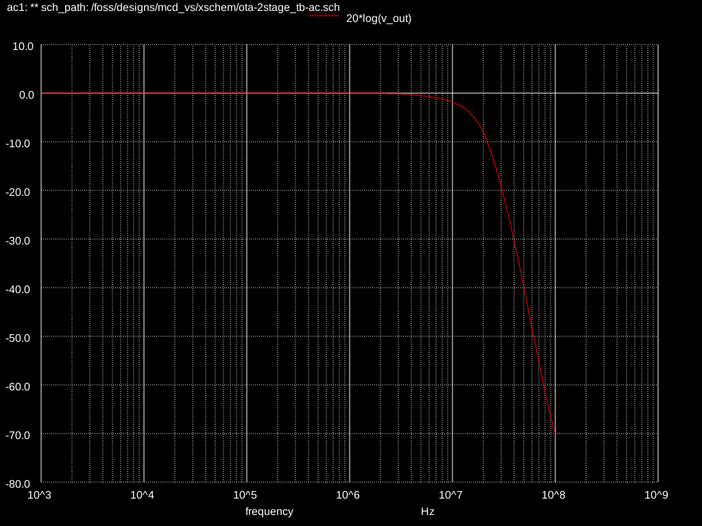
The AC characterization plots confirm an exceptionally clean frequency roll-off profile:
Unity-Gain Bandwidth (\(\text{UGBW}\)): The simulated crossover frequency measures safely above the \(10\text{ MHz}\) minimum requirement.
Loop Stability: Thanks to the Left-Half Plane (LHP) zero tracking added by the \(24\text{ k}\Omega\) nulling resistor ensuring no risk of ringing or oscillation.
Figure 6: 2-Stage OTA AC response.
5.7.2.2 2. Transient and Noise Fidelity
The transient step response simulation (ota-2stage_tb-trans.sch) shows a well-behaved, symmetric settling behavior with minimal overshoot.
The noise simulation (ota-2stage_tb-noise.sch) verifies that the input-referred noise voltage is kept low.
5.8 Sallen-Key Low-Pass Filter Integration
To evaluate the 2-stage Miller OTA within its intended system environment, it was integrated into a 2nd-order Sallen-Key Active Low-Pass Filter (LPF). The target design metric requires a strict \(-6\text{ dB}\) i.e \(Q\) = 0.5 cutoff frequency (\(f_{\mathrm{c}}\)) at exactly \(10\text{ kHz}\).
5.8.1 Passive Network Synthesis & Load Matching
Initial design attempts using standard textbook equal-component formulas yielded impractical results. To synthesize realistic on-chip values, the Okawa-Denshi Active Filter Design Tool(Okawa Electric Design 2026) was utilized to compute a the requires R and C values.
By setting the targeted performance constraints (\(f_{\mathrm{c}} = 10\text{ kHz}\)) and intentionally mapping the capacitor values to align with the OTA’s engineered load limit (\(C_{\mathrm{load}} = 1\text{ pF}\)), the network parameters were locked in:
With the synthesized asymmetric resistor network implemented in the Xschem testbench , the active filter architecture functions exactly as intended:
Frequency Tuning: The ac responce successfully achieves a stable attenuation slope with the desired \(-6\text{ dB}\) cross-over breakpoint localized around \(10\text{ kHz}\).
NoteVerification Testbench Workspace
All verification testbenches are present in the ./xschem workspace directory. Each setup used the exact same core ota-2stage.sym symbol, relying on the asymmetric impedance matching profiles calculated from the Okawa-Denshi design tool (Okawa Electric Design 2026):
ota-2stage_tb-sk-lpf.sch, ota-2stage_tb-sk-hpf.sch, ota-2stage_tb-lr2.sch and ota-2stage_tb-biquad.sch
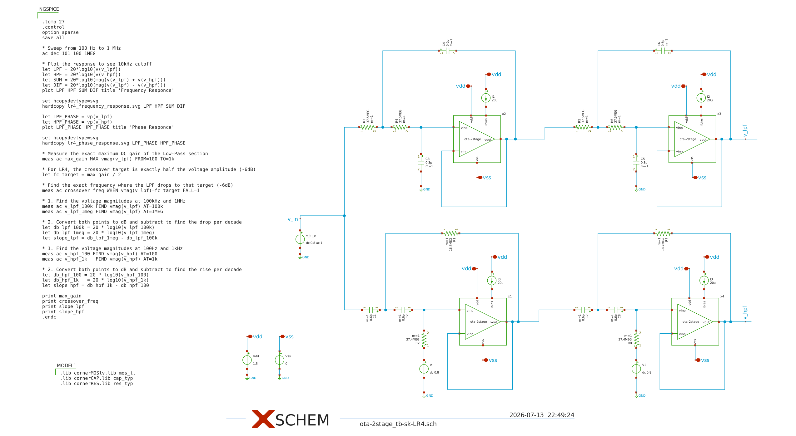
In addition to the two-stage OTA design, a fourth-order Linkwitz–Riley (LR4) crossover filter was implemented to investigate higher-order active filter design. The Linkwitz–Riley crossover is widely used in audio applications because it provides a flat summed frequency response when the low-pass and high-pass outputs are combined.
An LR4 crossover is obtained by cascading two identical second-order Butterworth filter sections. Since a second-order Butterworth filter has a quality factor
\[Q = \frac{1}{\sqrt{2}}\approx0.707\]
each stage was implemented using a Sallen–Key topology with a cutoff frequency of 10 kHz. The output of the first stage was connected directly to the input of the second stage, resulting in a fourth-order response.
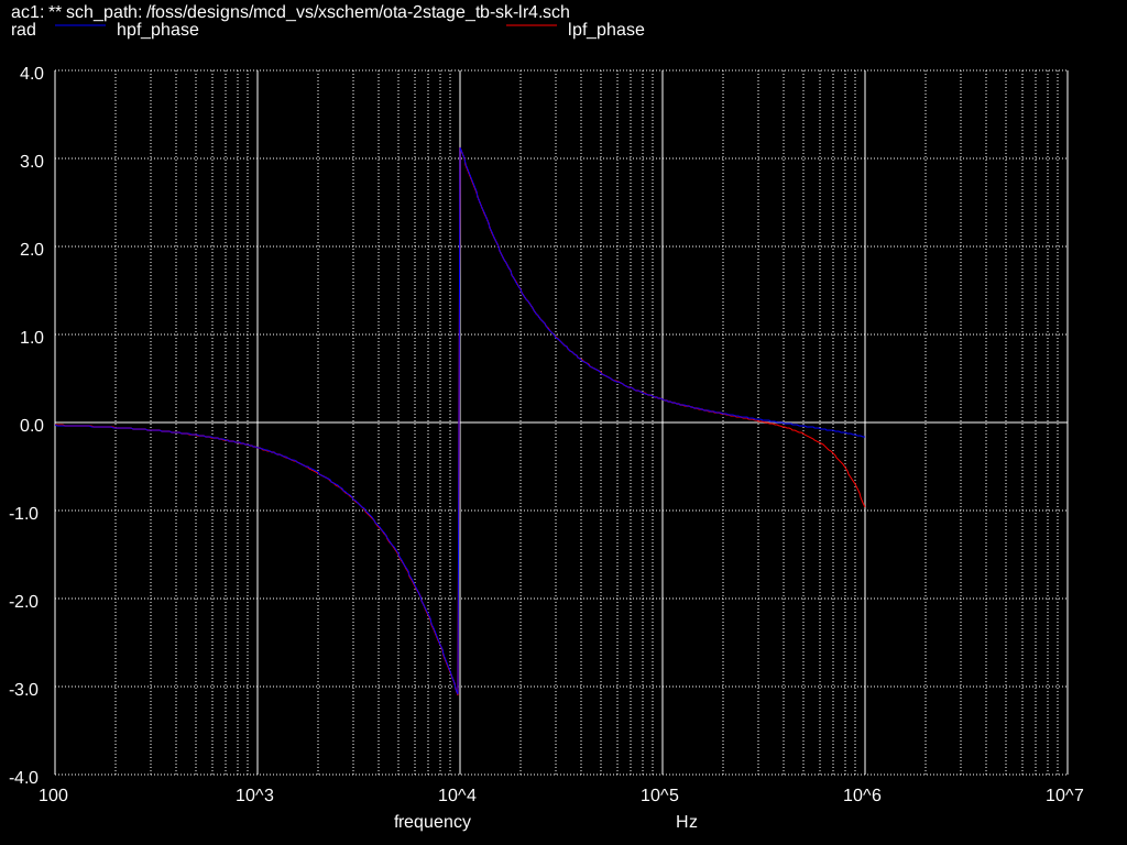
The same design procedure was followed for both the low-pass and high-pass branches. A common input signal was applied to both branches, and the individual frequency responses were simulated.
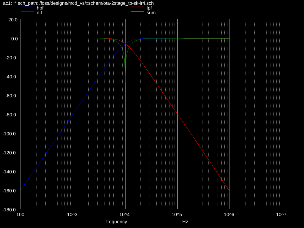
The resulting LR4 crossover exhibits the following characteristics:
Fourth-order response (80 dB/decade roll-off)
Cutoff frequency of 10 kHz
−6 dB gain at the crossover frequency
Flat summed response when the low-pass and high-pass outputs are combined
The component values are again derived from (Okawa Electric Design 2026) tool and the values used are shown in the table below.
6.1 Component values for the Linkwitz–Riley crossover
Component
Stage 1 LPF
Stage 2 LPF
Stage 1 HPF
Stage 2 HPF
R1
37.5 M\(\Omega\)
37.5 M\(\Omega\)
18.7 M\(\Omega\)
18.7 M\(\Omega\)
R2
37.5 M\(\Omega\)
37.5 M\(\Omega\)
37.4 M\(\Omega\)
37.4 M\(\Omega\)
C1
0.6 pF
0.6 pF
0.6 pF
0.6 pF
C2
0.3 pF
0.3 pF
0.6 pF
0.6 pF
Cutoff Frequency
10 kHz
10 kHz
10 kHz
10 kHz
Quality Factor (Q)
0.707
0.707
0.707
0.707
6.2 Simulation Environment Setup
The core filter design testbench schematic using the same ota-2stage.sym is present in ota-2stage_tb-sk-LR4.sch which is shown below in figure Figure 7
7 Process, Voltage, Temperature (PVT) and Monte Carlo (MC) Verification
7.1 Methodology and Objectives (Why it is Required)
A nominal circuit simulation operating solely at typical-typical (TT) manufacturing process parameters, fixed nominal supply voltages, and a constant room temperature (\(27^\circ\text{C}\)) provides an incomplete representation of real-world silicon performance. To guarantee high-yield manufacturability and operational robustness, the design must be validated against random environmental fluctuations and process parameters:
Environmental and Operational Variations (Voltage and Temperature): Power supply networks experience dynamic regulation tolerances, and environmental operating temperatures shift based on load and ambient conditions. The circuit must preserve properties across these extreme shifts (Pretl et al. 2026).
Systemic Manufacturing Excursions (Process Corners): Standard wafer fabrication introduces predictable deviations in threshold voltages (\(V_{\text{th}}\)), oxide thicknesses (\(t_{\text{ox}}\)), and carrier mobilities (\(\mu\)). Foundries quantify these boundaries through five discrete device corners: TT (Typical-Typical), SS (Slow-Slow), SF (Slow-Fast), FS (Fast-Slow), and FF (Fast-Fast) (Pretl et al. 2026).
Random Local Mismatch (Monte Carlo): Distinct from macroscopic wafer-to-wafer process variations, adjacent transistors on the same die experience microscopic, localized geometric differences (such as edge roughness or local dopant fluctuations). This mismatch induces random offsets, altering matching-critical parameters like input-pair symmetry, open-loop gain uniformity, and filter pole stability (Pretl et al. 2026).
Evaluating every combination of these variables creates a vast, multi-dimensional simulation space that must be systematically evaluated against pass/fail design metrics.
7.2 Implementation Framework (How it is Executed)
To efficiently execute this extensive matrix without relying on manual, error-prone testbench modifications, the verification architecture utilizes CACE (Circuit Automatic Characterization Engine).
CACE acts as an automated simulation runner that structures, parallelizes, and sweeps the design space via a unified, programmatically driven pipeline:
WarningRunning CACE Simulation
The CACE simulation run can be started with
cace cace/lpf-ota-2stage.yaml
The simulation results are then placed into the cace/_docs folder. If in addition to the default Markdown report an HTML output is needed for easier review then using Pandoc it can be easily converted and viewed with with
After a successful run, a documentation is automatically generated. The result of a full run of this 2 stage ota is presented here:
Note 1: CACE Summary for 2-Stage-OTA and LR4 filter
8 CACE Summary for ota-2stage
netlist source: schematic
Parameter
Tool
Result
Min Limit
Min Value
Typ Target
Typ Value
Max Limit
Max Value
Status
Output voltage ratio
ngspice
gain
0.97 V/V
1.003 V/V
any
1.004 V/V
1.03 V/V
1.007 V/V
Pass ✅
Bandwidth
ngspice
bw
10e6 Hz
10622800.000 Hz
any
18524800.000 Hz
any
35621100.000 Hz
Pass ✅
Output voltage ratio (MC)
ngspice
gain_mc
any
1.003 V/V
any
1.004 V/V
any
1.004 V/V
Pass ✅
Bandwidth (MC)
ngspice
bw_mc
10e6 Hz
17893700.000 Hz
any
18574000.000 Hz
any
19314700.000 Hz
Pass ✅
Output noise
ngspice
noise
any
0.171 mV
any
0.182 mV
1 mV
0.217 mV
Pass ✅
Settling time
ngspice
tsettle
any
0.177 us
any
0.189 us
10 us
0.199 us
Pass ✅
Passband Gain LPF
ngspice
gain
0.95 V/V
1.002 V/V
any
1.003 V/V
1.03 V/V
1.006 V/V
Pass ✅
Cutoff Frequency LPF (-3dB)
ngspice
fc
9.5e3 Hz
9841.100 Hz
10.0e3 Hz
9926.370 Hz
10.5e3 Hz
10430.500 Hz
Pass ✅
Passband Gain LPF (MC)
ngspice
gain_mc
any
1.001 V/V
any
1.003 V/V
any
1.004 V/V
Pass ✅
Cutoff Frequency LPF (MC)
ngspice
fc_mc
9.5e3 Hz
9917.100 Hz
10e3 Hz
9928.145 Hz
10.5e3 Hz
9935.940 Hz
Pass ✅
Output noise LPF
ngspice
noise
any
0.150 mV
any
0.172 mV
5.0 mV
0.220 mV
Pass ✅
Settling time LPF
ngspice
tsettle
any
46.271 us
150 us
49.571 us
400 us
52.504 us
Pass ✅
Passband Gain LR4 LPF
ngspice
gain_lpf
0.95 V/V
1.003 V/V
any
1.007 V/V
1.15 V/V
1.129 V/V
Pass ✅
Passband Gain LR4 HPF
ngspice
gain_hpf
0.95 V/V
0.964 V/V
any
0.982 V/V
1.15 V/V
1.088 V/V
Pass ✅
Cutoff Frequency LPF (-3dB)
ngspice
fc_lpf
9.4e3 Hz
9842.690 Hz
10.0e3 Hz
9926.940 Hz
10.5e3 Hz
10477.200 Hz
Pass ✅
Cutoff Frequency HPF (-3dB)
ngspice
fc_hpf
9.4e3 Hz
9418.250 Hz
10.0e3 Hz
9925.680 Hz
10.5e3 Hz
9949.830 Hz
Pass ✅
Phase Mismatch LPR4
ngspice
phase_error
0 °
0.006 °
0 °
0.007 °
5 °
0.008 °
Pass ✅
Output noise LR4 LPF
ngspice
noise_lpf
any
0.181 mV
any
0.208 mV
5.0 mV
0.277 mV
Pass ✅
Output noise LR4 HPF
ngspice
noise_hpf
any
0.193 mV
any
0.222 mV
5.0 mV
0.292 mV
Pass ✅
Settling time LR4 LPF
ngspice
tsettle_lpf
any
143.978 us
150 us
147.826 us
280 us
149.604 us
Pass ✅
Settling time LR4 HPF
ngspice
tsettle_hpf
any
39.067 us
150 us
39.551 us
280 us
41.721 us
Pass ✅
8.1 Plots
8.2 gain_vs_temp
gain_vs_temp
8.3 gain_vs_vin
gain_vs_vin
8.4 gain_vs_vdd
gain_vs_vdd
8.5 gain_vs_corner
gain_vs_corner
8.6 bw_vs_temp
bw_vs_temp
8.7 bw_vs_vin
bw_vs_vin
8.8 bw_vs_vdd
bw_vs_vdd
8.9 bw_vs_corner
bw_vs_corner
8.10 gain_mc
gain_mc
8.11 bw_mc
bw_mc
8.12 noise_vs_temp
noise_vs_temp
8.13 noise_vs_vin
noise_vs_vin
8.14 noise_vs_vdd
noise_vs_vdd
8.15 noise_vs_corner
noise_vs_corner
8.16 settling_vs_temp
settling_vs_temp
8.17 settling_vs_vin
settling_vs_vin
8.18 settling_vs_vdd
settling_vs_vdd
8.19 settling_vs_corner
settling_vs_corner
8.20 gain_vs_temp_lpf
gain_vs_temp_lpf
8.21 gain_vs_vin_lpf
gain_vs_vin_lpf
8.22 gain_vs_vdd_lpf
gain_vs_vdd_lpf
8.23 gain_vs_corner_lpf
gain_vs_corner_lpf
8.24 fc_vs_temp_lpf
fc_vs_temp_lpf
8.25 fc_vs_vin_lpf
fc_vs_vin_lpf
8.26 fc_vs_vdd_lpf
fc_vs_vdd_lpf
8.27 fc_vs_corner_lpf
fc_vs_corner_lpf
8.28 gain_mc_lpf
gain_mc_lpf
8.29 fc_mc_lpf
fc_mc_lpf
8.30 noise_vs_temp_lpf
noise_vs_temp_lpf
8.31 noise_vs_vin_lpf
noise_vs_vin_lpf
8.32 noise_vs_vdd_lpf
noise_vs_vdd_lpf
8.33 noise_vs_corner_lpf
noise_vs_corner_lpf
8.34 settling_vs_temp_lpf
settling_vs_temp_lpf
8.35 settling_vs_vin_lpf
settling_vs_vin_lpf
8.36 settling_vs_vdd_lpf
settling_vs_vdd_lpf
8.37 settling_vs_corner_lpf
settling_vs_corner_lpf
8.38 gain_vs_temp_lr4_lpf
gain_vs_temp_lr4_lpf
8.39 gain_vs_vin_lr4_lpf
gain_vs_vin_lr4_lpf
8.40 gain_vs_vdd_lr4_lpf
gain_vs_vdd_lr4_lpf
8.41 gain_vs_corner_lr4_lpf
gain_vs_corner_lr4_lpf
8.42 fc_vs_temp_lr4_lpf
fc_vs_temp_lr4_lpf
8.43 fc_vs_vin_lr4_lpf
fc_vs_vin_lr4_lpf
8.44 fc_vs_vdd_lr4_lpf
fc_vs_vdd_lr4_lpf
8.45 fc_vs_corner_lr4_lpf
fc_vs_corner_lr4_lpf
8.46 gain_vs_temp_lr4_hpf
gain_vs_temp_lr4_hpf
8.47 gain_vs_vin_lr4_hpf
gain_vs_vin_lr4_hpf
8.48 gain_vs_vdd_lr4_hpf
gain_vs_vdd_lr4_hpf
8.49 gain_vs_corner_lr4_hpf
gain_vs_corner_lr4_hpf
8.50 fc_vs_temp_lr4_hpf
fc_vs_temp_lr4_hpf
8.51 fc_vs_vin_lr4_hpf
fc_vs_vin_lr4_hpf
8.52 fc_vs_vdd_lr4_hpf
fc_vs_vdd_lr4_hpf
8.53 fc_vs_corner_lr4_hpf
fc_vs_corner_lr4_hpf
8.54 phase_error_vs_temp
phase_error_vs_temp
8.55 phase_error_vs_corner
phase_error_vs_corner
8.56 noise_vs_temp_lpf
noise_vs_temp_lpf
8.57 noise_vs_vin_lpf
noise_vs_vin_lpf
8.58 noise_vs_vdd_lpf
noise_vs_vdd_lpf
8.59 noise_vs_corner_lpf
noise_vs_corner_lpf
8.60 noise_vs_temp_hpf
noise_vs_temp_hpf
8.61 noise_vs_vin_hpf
noise_vs_vin_hpf
8.62 noise_vs_vdd_hpf
noise_vs_vdd_hpf
8.63 noise_vs_corner_hpf
noise_vs_corner_hpf
8.64 settling_vs_temp_lr4_lpf
settling_vs_temp_lr4_lpf
8.65 settling_vs_vin_lr4_lpf
settling_vs_vin_lr4_lpf
8.66 settling_vs_vdd_lr4_lpf
settling_vs_vdd_lr4_lpf
8.67 settling_vs_corner_lr4_lpf
settling_vs_corner_lr4_lpf
8.68 settling_vs_temp_lr4_hpf
settling_vs_temp_lr4_hpf
8.69 settling_vs_vin_lr4_hpf
settling_vs_vin_lr4_hpf
8.70 settling_vs_vdd_lr4_hpf
settling_vs_vdd_lr4_hpf
8.71 settling_vs_corner_lr4_hpf
settling_vs_corner_lr4_hpf
9 PVT Simulation Analysis
Looking at the CACE report in Note 1, we see that (luckily) the specification is met for all parameters. This is great news! We now have a design that we carefully simulated across PVT and other corners and that is ready for layout.
9.1 Monte Carlo Simulation Analysis
Looking at the CACE report in Note 1, we see that the output voltage specification is not met. We should now go back and change the transistor sizing (increasing \(L\) while keeping the \(g_m/I_D\) values). Likely we will find that some performance parameters are now deteriorating due to the increased MOSFET dimensions, and we need to iterate until all performance metrics are met.
It is not unusual that the power consumption now increases, as we have to increase the size of the MOSFETs for matching, and these larger MOSFETs increase the parasitic capacitances which in turn lead to larger power consumption to keep the required bandwidth by increasing the \(g_m\).
10 Declaration of Generative AI Assistance
In accordance with academic integrity and transparency guidelines, the following generative AI tools were utilized during the development and documentation of this project:
NotebookLM (Google): Employed as an interactive literature-analysis and educational tool to support the conceptual understanding of the two-stage Operational Transconductance Amplifier (OTA) topology and to assist in verifying the mathematical formulations governing transconductance (\(g_m\)) Miller capacitance \(C_M\) and Null resistor \(R_Z\) calculations (Repaka and Sunkari 2026).
Large Language Models (LLMs): Utilized strictly as editing and writing assistants to perform text paraphrasing, sentence restructuring, and grammar corrections to ensure high-quality, professional technical communication.
All primary circuit design, schematics in Xschem, simulation configurations, and engineering decision-making remain the original work of the authors.
Lenka, Trupti Ranjan, Durgamadhab Misra, and Arindam Biswas, eds. 2022. Micro and Nanoelectronics Devices, Circuits and Systems: Select Proceedings of MNDCS 2021. Vol. 781. Lecture Notes in Electrical Engineering. Springer Singapore. https://doi.org/10.1007/978-981-16-3767-4.
Meiners, Mirco. 2026. Lecture Notes on Analogue and Mixed-Signal Circuit Design. Hochschule Bremen; Lecture Script, Hochschule Bremen.
Nagulapalli, Rajasekhar, K. Hayatleh, and B. Seetharamulu. 2019. “A Low Power Miller Compensation Technique for Two Stage Op-Amp in 65nm CMOS Technology.”International Conference on Computing, Communication and Networking Technologies (ICCCNT), July. https://doi.org/10.1109/ICCCNT45670.2019.8944553.